
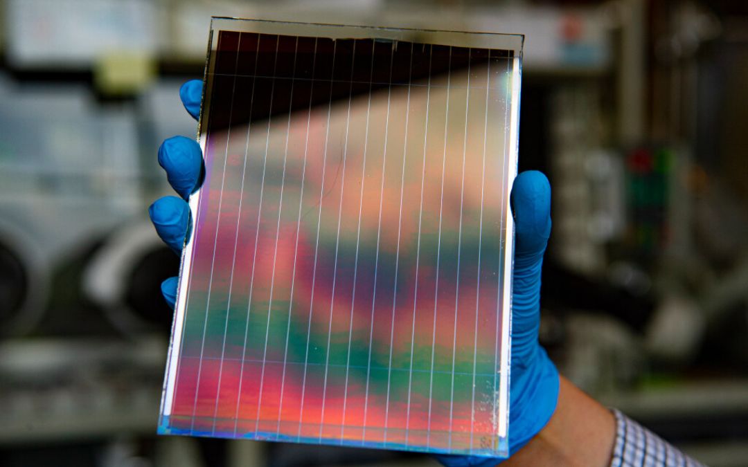
Perovskite/silicon tandem solar cells achieved 30.6% efficiency over an area of 207.87 cm². The result achieved by the team described in Nature Energy is important not only because of the efficiency itself. Much more important is that the solution retained high performance after the device area was increased. The titanium oxynitride layer used in the device is designed to conduct charges, limit optical losses, and improve the quality of the interface between successive cell layers.
In the laboratory, it is relatively easy to achieve high efficiency on a small device. It is much harder to transfer such a result to a larger area, because as the scale increases, the importance of material nonuniformity, resistance, defects, and losses at the connections between layers also increases. In the case of perovskite/silicon tandems, the problem is particularly significant because the structure combines two different subcells and requires their precise electrical and optical connection. The authors of the study identify the recombination layer as one of the elements limiting the further development of such devices.
The results demonstrate scaling that is difficult to reduce to another laboratory record. For a device with an area of 1 cm², an efficiency of 33.3% was achieved, while for a device with an area of 207.87 cm², the figure was 30.6%. The difference is therefore 2.7 percentage points. Relative to the result from the smallest device, this represents a drop of around 8%, despite an increase in the active area by more than two hundred times. It is this second figure that is important from the perspective of production technology.
A perovskite/silicon tandem uses two active layers that absorb different parts of the solar spectrum. Silicon forms the lower part of the structure, while perovskite forms the upper layer, with properties that allow an additional part of the radiation to be used. This combination makes it possible to move beyond the limitations of conventional cells with a single absorbing material.
There is, however, an area between these parts that has to perform several tasks at the same time. The recombination layer should enable efficient connection of charges from both subcells, it cannot excessively block the light reaching the lower cell, and it must provide a stable interface for the subsequent layers. Any compromise at this point can translate into a reduction in voltage, fill factor, or light utilisation.
Existing solutions include transparent conductors containing indium. Their advantages are good conductivity and transparency, but the use of indium raises questions about the cost and availability of the raw material. An alternative can be silicon based interconnections, but these also introduce their own optical losses. It is precisely between these requirements that the authors have placed titanium oxynitride, designated as TiOₓNᵧ.
Titanium oxynitride is designed to perform several functions at once
The material was not treated solely as a conductive intermediate layer. According to the authors, its structure enables effective recombination of charge carriers in the vertical direction, limits lateral charge flow, and at the same time creates sites that enable the anchoring of self assembled monolayers.
The latter is important because a tandem is not simply about finding a material that conducts electricity. The surface must also interact properly with the subsequent layers of the device. If the connection at the material interface is unstable or nonuniform, a larger device area begins to reveal problems that may remain practically invisible on a small sample.
In the case of TiOₓNᵧ, the authors point to the possibility of solving several problems simultaneously. The layer is intended to be conductive, limit losses associated with lateral flow, and provide a suitable environment for a self assembled layer. At the same time, the material contains no indium, which could be important when designing a production process aimed at a larger scale.
30.6% is more important than 33.3%
In photovoltaic research, a record achieved over an area of one square centimetre is relatively easy to highlight, but its industrial significance is limited if efficiency drops sharply as the area increases. A larger device requires uniform deposition of materials, defect control, and the limitation of resistive and optical losses across the entire surface.
In this case, the difference between 33.3% and 30.6% is noticeable, but it does not undermine the result achieved on the larger device. The area of 207.87 cm² is more than 200 times larger than the area of the device used to achieve the highest efficiency. This makes it possible to test whether the developed architecture retains its properties when the importance of process uniformity increases.
This does not mean, however, that a module ready for installation on roofs or solar farms has already been produced. 207.87 cm² is still the area of a research device. The significance of the result lies elsewhere: it shows that the problem of the recombination layer can already be studied at a scale much closer to production requirements than in the case of conventional laboratory samples. The publication itself presents the result as an achievement for an industrial size device and as a step towards scalable interconnection for tandems.
The significance of tandems does not end with the efficiency record itself. If the technology can actually achieve higher efficiency over large areas, the amount of energy that can be generated per unit area of an installation changes.
For photovoltaics, this is a parameter with system level significance. Higher energy production from one square metre can reduce the area needed to achieve a given power output, reduce the number of support structures and connections required to build an installation with a given production capacity, and in some locations also reduce pressure related to land availability. This does not automatically mean a lower cost for the entire system, because the economics also depend on material prices, production speed, durability, manufacturing yield, and the costs of the other components of the installation.
This is precisely why the 30.6% result should be considered together with information about the device area. Efficiency alone does not yet indicate whether the technology will be cheaper than existing solutions. It does, however, show that the potential advantage of tandems does not necessarily have to be limited to very small laboratory samples.
Indium is not the only problem the researchers addressed
The use of TiOₓNᵧ may also have significance from a materials perspective. The authors point out that current transparent conductive layers containing indium have limitations related to cost and the sustainable use of raw materials. Replacing them with an indium free material does not solve all the problems associated with tandem production, but it removes one element of material dependence.
At the same time, the new layer is intended to avoid the classic compromise in which improving electrical properties comes at the expense of light transmission. This is particularly important for a tandem because light that is not used by the upper perovskite layer should reach the silicon cell underneath it. An intermediate layer that was too absorptive would therefore reduce the potential benefit of combining the two materials.
The authors also point to the limitation of lateral charge flow. This is important when increasing the area, because defects and local conduction paths can lead to losses that are less significant in a small device but begin to limit the performance of the entire structure over a larger area.
The next stage is no longer a record, but production
The publication in Nature Energy shows that the development of perovskite/silicon tandems is moving from the question of maximum efficiency in a small cell towards the question of maintaining high efficiency over a larger area. The use of TiOₓNᵧ is interesting precisely because a single layer has been designed to address several problems at the same time: conductivity, recombination, limiting optical losses, interface control, and the elimination of indium.
There remains, however, a fundamental difference between a device with an area of 207.87 cm² and a full size photovoltaic module. Industrial production requires not only maintaining performance over an even larger area, but also high manufacturing yield, process repeatability, adequate durability, and the ability to carry out subsequent stages at costs acceptable to the market. The publication therefore primarily shows that one of the technological barriers can be pushed further, rather than that perovskite/silicon tandem technology is already a ready alternative to current modules.